
For years, whispers about the death of Moore’s Law have echoed across semiconductor fabs, R&D labs, and strategy meetings. Each technological plateau, each physical limit, each economic hurdle seemed like it might be the final nail in the coffin. Yet, despite these obstacles, the industry continues to innovate, adapt, and stretch the meaning of Moore’s Law into new dimensions. Erik Hosler, a semiconductor strategist known for his insight into cross-sector development and long-term scaling outlooks, reminds us that the survival of Moore’s Law was never guaranteed.
In fact, the question may no longer be whether Moore’s Law is alive or dead. It may be whether the industry has learned how to outmaneuver its demise. With traditional feature scaling slowing down, engineers have turned to new materials, smarter design strategies, AI-enabled fabs, and unconventional architectures to keep the performance curve moving upward. And yet, despite these advances, the case remains unsolved. Moore’s Law is no longer a steady climb. It is a battlefield of breakthroughs, a series of hard-won victories against physics, cost, and complexity.
A Law Rewritten, Not Replaced
Moore’s Law began as an observation of transistors doubling every two years, driven by advances in lithography. Shrinking features allowed more logic per square millimeter, which translated into faster and more power-efficient chips.
But in recent years, pure dimensional scaling has slowed. The economics of advanced nodes, the stochastics of EUV lithography, and the difficulty of further shrinking gate lengths have forced the industry to think beyond traditional lithographic limits.
Instead of abandoning the principle altogether, chipmakers have redefined the law. Today, the spirit of Moore’s Law lives on in system-level performance, energy efficiency, and integration density, even if transistor counts no longer double on cue.
The conversation has shifted from raw scaling to meaningful scaling, where development at every layer of the stack, from design and packaging to materials and algorithms, contributes to continued progress.
Evidence of Life in New Directions
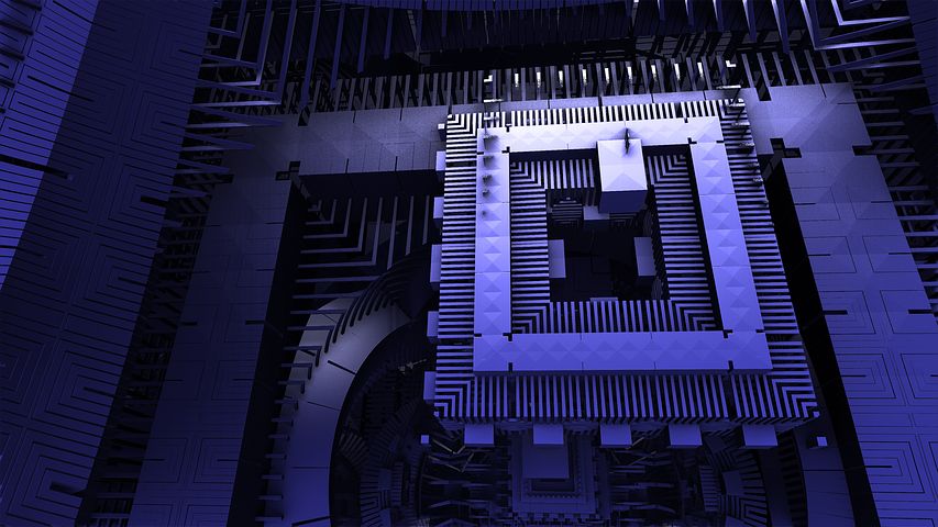
Though planar transistor scaling has slowed, breakthroughs in other areas suggest that Moore’s Law still has momentum. Gate-all-around FETs, 3D stacked architectures, and chiplets are breathing new life into performance-per-area metrics.
In tandem, design tools have become more powerful and data-driven. Engineers can now simulate the entire process flow before a chip is ever fabricated, allowing for better variability control and tighter optimization of layout and logic.
Advanced packaging is also vital. With technologies like 2.5D integration, through-silicon vias, and interposer-based design, chipmakers are now able to achieve higher performance by co-packaging multiple dies, each optimized for a specific function.
While these approaches are not purely lithographic, they continue Moore’s mission of packing more performance into less space with smarter engineering.
The Role of Lithography in the Open Case
Still, lithography remains central to the story. EUV scanners with 0.33 NA opened the door to 7 nm and 5 nm nodes. Now, high-NA EUV systems promise to extend that further, potentially enabling 2 nm and beyond with better resolution and fewer patterning steps.
However, the lithographic process is becoming more complex. Photoresist chemistry must improve to deal with low photon doses, and metrology must develop to monitor sub-nanometer features with higher precision. Defect control has become critical at every layer.
There are also growing dependencies between lithography and etch processes. Pattern fidelity is no longer the result of exposure alone. It is the product of coordinated precision across toolsets, materials, and process flows.
This complexity is why some experts refer to the continued pursuit of Moore’s Law as a mystery, one that changes shape as new techniques are introduced.
The Scene of the Struggle
For some, Moore’s Law has already been “murdered.” They point to the slowing of transistor doubling, the astronomical costs of new nodes, and the growing length of design cycles as evidence of its demise.
But the persistence of progress suggests a more nuanced reality. The murder scene is messy. There is no smoking gun. Instead, there are competing theories, plausible alibis, and new evidence emerging every year.
The panelists at SPIE’s Advanced Lithography symposium embraced this ambiguity. Rather than declaring Moore’s Law dead or alive, they explored what it might become. Would spectral metrology save it? By design ingenuity? By process control powered by AI?
One perspective stood out clearly. Even if Moore’s Law no longer follows its original timeline, it still defines a direction, one that continues to push the industry toward creative and collaborative solutions.
Beyond a Single Discipline
The truth behind Moore’s Law’s future lies in the convergence of efforts across many fields. Physics alone cannot solve the problem. Neither can materials science nor software. Progress now depends on unified development.
As pressure mounts to extend scaling, companies are collaborating in unprecedented ways. Lithographers are working with materials scientists, fab operators are partnering with AI specialists, and system architects are coordinating with packaging engineers.
Leading-edge fabs have become ecosystems of synchronized problem-solving. Real-time process feedback, data-driven optimization, and cross-functional simulation are now standard. This layered, multi-disciplinary model reflects how Moore’s Law has developed. Erik Hosler observes, “But avoiding the death of Moore’s Law won’t be easy.” Indeed, the path forward is not guaranteed. It demands investment, collaboration, and a willingness to challenge conventions at every level of the semiconductor process.
The Case for Keeping It Alive
Despite the headwinds, the motivation to preserve Moore’s Law remains strong. It continues to serve as a rallying cry for innovation and a benchmark for progress. Even as the pace of advancement slows, the aspiration to do more with less is as relevant as ever.
Moore’s Law inspires roadmaps, aligns R&D priorities, and shapes expectations for performance per watt and transistor cost. Its influence extends beyond chipmakers, touching software developers, system integrators, and end users alike.
Importantly, it continues to develop. Moore’s Law may no longer refer strictly to transistor doubling. Instead, it represents a mindset, a shared belief in the power of relentless optimization and clever engineering.
The Verdict Is Still Out
Moore’s Law has not been murdered. It has been transformed. What began as a simple projection has grown into a dynamic, multi-faceted challenge that requires every corner of the semiconductor world to participate.
The lithography floor may look different today than it did two decades ago, but its role remains central to the industry’s ambition. Whether through better optics, smarter materials, tighter integration, or more collaborative strategies, the search for continued scaling is still very much alive. And like any good mystery, the end may not be final. It may simply be the start of a new chapter, one written by the next generation of technologists who refuse to let Moore’s Law rest in peace.
Comments are closed.